- Meeting
- 2017/ 1/16 - 18 AFAD at Lanzhou
- 2017/ 2/27-3/4 INSTR2017 at Novosibirsk
- 2017/ 5/9-12 TYL workshop at Strasburg
- 2017/ 5/22-26 TIPP2017 at Beijing (not IHEP)
- 2017/ 7/3-7 NDIP 17 at France
- November 7-10, 2016
- 31st International Congress on High-Speed Imaging and Photonics(31st ICHSIP),Osaka, Japan
- 2014.5.19 SOIpix topics;
- Togo Kudo, Kazuo Kobayashi, Shun Ono, Takeo Watanabe, Hiroo Kinoshita,Masao Okihara, and Takaki Hatsui, et.al, "Development of Experimental Methodology for Highly Efficient Wafer-Level valuation of X-Ray Radiation Effects on Semiconductor Devices",IEEE Transactions on Nuclear Science,Vol.61,Issue 3,pp1444-pp1450,(2014)
- 2014.3.14
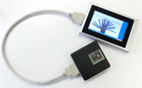
- SOI Portable Radiation imaging Terminal. "SPRiT"
2013.10.01 from Annual Rept.-2012-
In FY2011, the KEK Detector Project started foucused overseas promotion. In June of that year, a delegate was sent to Germany and Poland to demonstrate the potential of the Silicon-On-Insulator (SOI) pixel sensor technology and to invite the colleagues in MPI, AGH-UST, and IFJ-PAN to join this project. In that summer, a visiting researcher from IHEP, Beijing collaborated with the KEK detector team for developing a sensor as well as electronics using an SOI technology. In September, the KEK Detector Project co-hosted the 2nd MPGD international conference in Kobe for discussing various topics related to the micro pattern gas detector; more than 60 foreign researchers attended this conference. A beam test on the MPGD system was conducted at the Rutherford Appleton Laboratory (RAL) in the UK, and the capability of this system as an excellent neutron detector was demonstrated. Similarly, the SOI project carried out a beam test at CERN in October to demonstrate that the performance of the SOI pixel sensor as a particle detector is unparalleled. In autumn, under the JSPS program, KEKDTP invited several young researchers from Southeast Asia to gain good experience in working with the detector R&D projects. There were also several exchanges with French researchers via TYL in activities related to the Liquid Xenon TPC and the Next-Generation Photon Sensor projects. In early February 2012, during the Asian Forum for Accelerator and Detector (AFAD) workshop held in Kolkata, we discussed with Indian institutes the prospect of promoting intensive collaborations on detector R&D. The SOI project held an international collaboration meeting at LBNL on 15 and 16 March; this meeting was attended by colleagues from 13 institutes across 6 countries, including three observers from PAL (Korea) who showed a strong interest in joining the collaboration. In the annual KEK-DESY collaboration meeting held in March, a special parallel session was conducted for focusing on the development of detector technology for particle/nuclear physics and photon science. This session stimulated greater collaborative effort in those fields.
- 2013.9
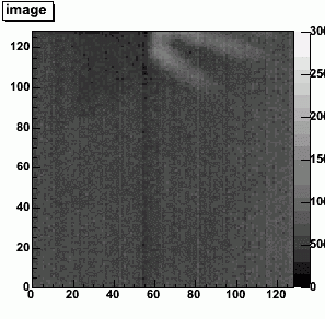
- An X-ray moving picture of a rotation chopper taken by the SOI pixel sensor.

2010.7.15 An advanced 2D detector for medical, materials and life sciences
One of the Detector Technology Project (DTP) groups at KEK has developed
multi-purpose, two-dimensional detector called a gas electron multiplier
(GEM) for use in small radiation-related experiments. The GEM’s good time-
resolution has also given birth to a new field of radiography, called energy-
selective radiography. Read here how GEM can play an important role in
neutron science, medical applications, and more.
2010.06.16 New network-based DAQ framework may simplify life for scientists
The data acquisition system (DAQ) team at KEK’s Detector Technology
Project is now offering the particle experiment community a standardized
data acquisition system (DAQ) framework of both hardware and software.
Learn here about the innovative, network-based readout electronics, and
the all-in-one DAQ-Middleware.
・Invitation message from JINST (Prof. Amos Breskin )
SOI Project of KEKDTP is introduced in LBL WEB site
Japan Science and Technology(JST) has approved SOI project of KEKDTP
as development of systems and technology for advanced measurement and analysis.Here is the WEB side. in Japanese
![]()
The first moving pictures by the new large SOI pixel 'CAMERA'