TYL-FJPPL Project: Development of Advanced Monolithic Pixel Detector
Last modified July 21, 2017
Project ID: D_RD_16
Members:
Summary of Project:
The next generation of lepton colliders (such as the ILC) requires a vertex detector with utmost precision, calling for tiny pixels located very close to the interaction point. The consecutive hit rate generated by the beam related background imposes the pixel read-out to be fast enough to keep the occupancy at an acceptable level. The consecutive complexity of the read-out circuitry, however, relies on a footprint which tends to conflict with the restricted pixel dimensions and can generate sizeable power consumption. The conflict is enhanced by material budget restrictions, which clearly favour monolithic devices instead of hybrid ones.
These observations have motivated a long-term development of various pixel technologies, among which several ones exploiting industrial CMOS processes. The latter have shown to be the most promising among all alternatives considered up to now. The most advanced R&D however did not yet fully solve the conflict between precision, read-out speed and power consumption. It is the objective of the present partnership to overcome the remaining obstacles, its ultimate goal being a single bunch crossing tagging capability with pixels providing a precision better than 3 μm.To reach these target values, the strategy will consist in combining the advantages of the CMOS and SOI technologies in a partnership between two teams concentrating the necessary know-how in both technologies.
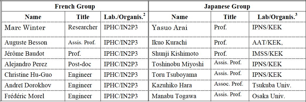
The IPHC group has a long history in developing monolithic CMOS Pixel Sensors (CPS). MIMOSA chips are used in a variety of devices, the PXL detector of the STAR experiment (Fig. 1) at BNL acting as a flagship for the benefits of CPS in charmed meson tagging, based on its recently completed 3 years long physics programme.
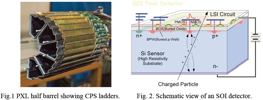
The Japanese group has been developing monolithic pixel sensors by using a Silicon-on-Insulator (SOI) technology. The SOI detector has both sensor and (CMOS) circuit layers in a wafer as shown in Fig. 2. The process is very flexible, providing great capabilities of developing new detectors. In addition to charged particle detection, both groups are also working for X-Ray detection.
Their partnership will reinforce the development of both technologies due to the enhanced chip designing and testing capabilities. Furthermore, both groups have established relationships with Chinese researcher groups, providing the opportunity of additional synergies.
Document
- May 11, 2017: Presentation by Y. Arai in TYL-FJPPL Workshop @ Strasbourg.
Contact
- Yasuo Arai (High Energy Accelerator Research Organization, KEK)

- Marc Winter (Institut Pluridisciplinaire Hubert Curien, IPHC/IN2P3)