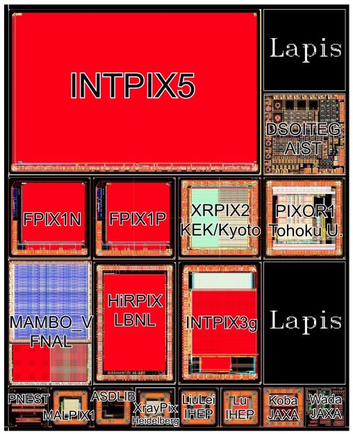
KEK-Lapis SOI Pixel Multi Project Wafer (MPW) run
Last modified Jan. 9, 2025, Y.Arai
 MX1501 SOI MPW run
----------------
*** Coming SOI MPW run Schedule: FY25-1 ***
----------------
We, KEK, are operating Multi Project Wafer (MPW) run of 0.2 um Silicon-On-Insulator (SOI) pixel process periodically
(~2 runs / year). This MPW run is open to academic users of all over the world. If you would like to join the MPW run, please send email to Yasuo Arai (yasuo.arai@kek.jp) .
[Brief summary of the SOI process]
Process : Lapis Semiconductor Fully-Depleted 0.2um SOI CMOS process.
Wires : 1 Poly + 5 metal layers.(minimum wire pitch is 0.58um)
Voltage : 1.8 V for core transistors, 1.8V/3.3 V for I/O transistors.
Transistors : Low threshold, High threshold, I/O, and DMOS
Options :
Creation of sensor diodes in handle wafer (p+ and n+ implantations).
MIM capacitor (1.5 fF/um2, minimum size 5um x 5um)
Poly resistor, lateral diode.
3D vertical integration option with T-micro u-bump technology(~5um pitch)
2 Buried p-well (p implant to handle wafer through surface Si)
3 Buried n-well (n implant to handle wafer through surface Si)
176 pins or 240 pins ceramic PGA package
CAD environment :
Cadence Virtuoso layout editor with parameterized cell.
HSPICE simulation model
Mentor Calibre Design Rule check
Star-RCXT RC Extraction
-----------------------
Past MPW runs
July 2023: MX2274
Nov. 2021: MX2263
........
-----------------------
Cost : ask to yasuo.arai
Related web page : http://rd.kek.jp/project/soi/
Contact : yasuo.arai at kek.jp
Go to SOI R&D TOP
 MX1501 SOI MPW run
 MX1501 SOI MPW run