|
3.5
Department of Advanced
Accelerator Technologies
Detector Technology Project Office
The KEK Detector Technology Project (KEKDTP) office is
now focusing on six R&D projects to enhance the level of
advanced detector technologies at KEK, to establish it as a
world leading accelerator laboratory.
In FY2016, the Silicon-On-Insulator (SOI) pixel project
moved to the stage of practical use. The SOI photon imaging
array sensor (SOPHIAS) detector developed for X-ray
imaging by the RIKEN group was used in several beam lines
at SPring-8 facility. The X-ray SOI pixel (XRPIX) detector
developed for X-ray astronomy by a Kyoto University group
achieved the highest ever energy resolution of 400 eV for an
X-ray with an energy of 13.95 keV by lowering the noise level
to around 10 electrons at a temperature of −60 °C. (->see more)
4.16 SOI pixel sensor opens a new era of particle and nuclear physics
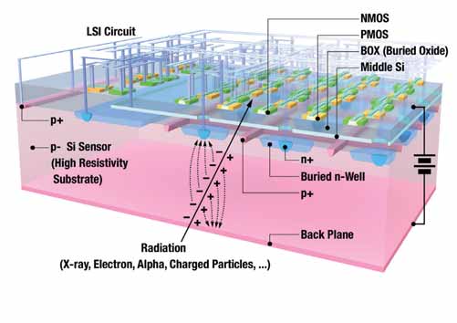
A pixel detector plays an important role in particle physics to study decay of short lived particles involving heavy quarks or the lepton with excellent time and spatial resolution under harsh radiation environment in a high luminosity particle accelerator. In silicon-on-insulator (SOI) technology, CMOS (complementary metal oxide semiconductor) circuits are fabricated on a thin SiO2 insulating layer (buried oxide, BOX) on the silicon substrate. As each circuit element like a transistor is isolated on BOX, parasitic capacitance and leakage current are minimized in an SOI circuit realizing an ideal characteristic beyond that of a normal CMOS. A pixel sensor using SOI technology (SOIPIX) would, therefore, serve as an excellent particle detector, where charges induced by radiation in the silicon substrate (bottom) are collected and processed in the CMOS circuit (top) on the BOX (Fig. 1). The small feature size of CMOS helps to realize high performance, monolithic pixel sensors. (->see more)

Fig. 1. Concept of the SOI pixel sensor.
|